1. Introduction
The increasing reliance on low-voltage direct current (DC) electronics in modern applications ranging from embedded systems and portable devices to laboratory equipment has heightened the importance of robust overvoltage protection mechanisms. Voltage irregularities, particularly in environments where both active and passive power sources are utilized, can significantly compromise system performance, reduce component lifespan, and lead to catastrophic device failures. Ensuring voltage stability across a wide input range has thus become a key design priority for circuit engineers. Traditional overvoltage protection strategies often rely on discrete components such as metal oxide varistors (MOVs), Zener diodes, and transient voltage suppression (TVS) diodes
| [1] | P. Sarajcev, A. Meglic, and R. Goic, “Lightning Overvoltage Protection of Step-Up Transformer Inside a Nacelle of Onshore New-Generation Wind Turbines,” Energies, vol. 14, no. 2, p. 322, Jan. 2021, https://doi.org/10.3390/en14020322 |
[1]
. While effective in many scenarios, these approaches can be limited in their ability to provide dynamic regulation across variable input conditions, particularly in compact or integrated designs. Moreover, many modern devices demand not only protection against voltage surges but also consistent operation under low-voltage conditions challenges those conventional methods alone may not adequately address
| [2] | J. Snodgrass and L. Xie, “Overvoltage analysis and protection of lightning arresters in distribution systems with distributed generation,” Int. J. Electr. Power Energy Syst., vol. 123, p. 106209, Dec. 2020, https://doi.org/10.1016/j.ijepes.2020.106209 |
[2]
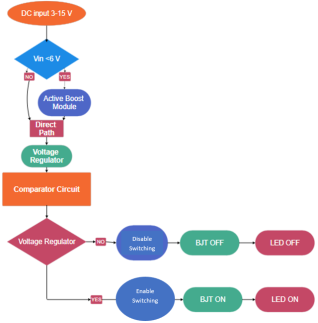
. In this work, we propose a comprehensive overvoltage protection circuit capable of operating within an input range of 3V to 30V. The design merges three essential sub-circuits into a unified architecture; (1) a boost converter, which activates when the input voltage drops below the critical 5V threshold, utilizing an astable multivibrator based on a 555 timer. (2) a voltage regulator, which ensures a steady 5V output irrespective of input fluctuations and (3) a comparator circuit, which continuously monitors the source voltage against a reference to detect and respond to overvoltage conditions. This integration of both passive and active components allows the system to dynamically adapt to varying power sources and provide stable, regulated output
| [3] | S. Molla, M. Shawon, M. Nawaj, and A. Emon, “Analysis of Aging Effect and Cell Balancing Problem of Lithium-Ion Battery,” J. Electr. Electron. Eng., vol. 13, no. 2, pp. 92-107, Mar. 2025, https://doi.org/10.11648/j.jeee.20251302.11 |
[3]
. The proposed circuit is particularly well-suited for applications where power sources may vary unpredictably, such as battery-powered systems, lab-scale prototypes, or field-deployable sensor networks. By leveraging well-established components in an innovative configuration, this design contributes to the broader field of power electronics by offering a scalable, efficient, and cost-effective solution for overvoltage protection
| [4] | E. Gómez-Luna, J. De La Cruz, and J. C. Vasquez, “New Approach for Validation of a Directional Overcurrent Protection Scheme in a Ring Distribution Network with Integration of Distributed Energy Resources Using Digital Twins,” Energies, vol. 17, no. 7, p. 1677, Apr. 2024, https://doi.org/10.3390/en17071677 |
[4]
.
Figure 1. Flowchart of the Proposed DC Overvoltage Protection System.
In the evolving landscape of modern electronics, low-voltage DC systems are increasingly employed in applications ranging from embedded devices and portable gadgets to laboratory instrumentation and sensor networks. These systems, while efficient and compact, are inherently sensitive to input voltage fluctuations, making them vulnerable to both undervoltage and overvoltage conditions
| [5] | A. P. Selvam and S. N. S. Al-Humairi, “The Impact of IoT and Sensor Integration on Real-Time Weather Monitoring Systems: A Systematic Review,” Nov. 10, 2023, Springer Science and Business Media LLC. https://doi.org/10.21203/rs.3.rs-3579172/v1 |
[5]
. Such irregularities especially in environments powered by passive sources like batteries or solar panels can severely compromise performance, reduce the lifespan of components, and in extreme cases, lead to system failure. Traditional overvoltage protection methods, including metal oxide varistors (MOVs), Zener diodes, and transient voltage suppression (TVS) devices, provide basic surge protection but are often limited by fixed threshold behavior and a lack of adaptability to variable input conditions. Moreover, many modern devices demand not only overvoltage protection but also functional stability under low-voltage operation requirements that are not fully addressed by conventional techniques
| [6] | R. He, Y. Jin, W. Hou, D. Luo, and S. Huang, “A capacitor overvoltage elimination strategy for reduced-voltage-sensor-based MMC,” Int. J. Electr. Power Energy Syst., vol. 132, p. 107181, Nov. 2021, https://doi.org/10.1016/j.ijepes.2021.107181 |
[6]
. To overcome these limitations, this research proposes a novel and integrated approach to overvoltage protection, specifically designed to operate across a wide DC input range of 3V to 30V. The system incorporates three critical sub-circuits a boost converter that activates below 5V input to elevate voltage using a astable multivibrator, a voltage regulator that maintains a consistent 5V output, and a comparator-based circuit that detects overvoltage and initiates load disconnection. This architecture ensures dynamic voltage handling, system adaptability, and load protection, making it highly suitable for both active (regulated) and passive (unregulated) power sources
. By merging stability, responsiveness, and protection into a single circuit, the proposed system contributes to the advancement of resilient power electronics, particularly in low-power, space-constrained, and field-deployable applications.
3. Methodology
This section outlines the systematic approach for designing and implementing a wide-input-range (3V-30V) DC overvoltage protection system, integrating boost conversion, voltage regulation, and comparator-based monitoring. The methodology is structured into design phases, component selection, simulation, prototyping, and testing.
3.1. Circuit Design Overview
The proposed circuit is structured to manage wide DC input voltages ranging from 3V to 30V and ensure a stable and protected 5V output for connected electronic devices. The design incorporates three main functional blocks each tailored to handle specific input conditions and ensure seamless operation of the protection mechanism
| [8] | Y. Deng et al., “Cluster analysis of cloud-to-ground lightning activities near transmission lines in typical terrains,” Electr. Power Syst. Res., vol. 225, p. 109876, Dec. 2023, https://doi.org/10.1016/j.epsr.2023.109876 |
[8]
. These include:
(i) A Boost Converter for low-voltage input handling,
(ii) A Voltage Regulation Stage for stabilized output, and
(iii) A Comparator-Based Protection Circuit for monitoring and response.
3.1.1. Boost Converter (DC-DC Step-Up Stage)
The boost converter increases the input voltage (when Vin<5V) to a higher level suitable for regulation. Where, Boosted output voltage (V
out), Input voltage (3-5V) (Vin), Duty cycle of PWM signal (0 < D < 1)
| [9] | M. Abolghasemi, I. Soltani, M. Shivaie, and H. Vahedi, “Recent advances of step-up multi-stage DC-DC converters: A review on classifications, structures and grid applications,” Energy Rep., vol. 13, pp. 3050-3081, Jun. 2025, https://doi.org/10.1016/j.egyr.2025.02.025 |
[9]
. Voltage Gain Equation,
Output Voltage:
Duty cycle (a value between 0 and 1 representing the fraction of time the switch is ON in one cycle).
As D increases, the output voltage increases, when D= 0.5, and as .
Minimum Inductance (Continuous Conduction Mode - CCM):
If inductance is below this value, the converter may enter Discontinuous Conduction Mode (DCM), which requires different analysis, Average Inductor Current:
This gives the average current flowing through the inductor, which is the same as the input current in CCM, Inductor Current Ripple:
The inductor current fluctuates in each cycle, Output Voltage Ripple:
This helps in selecting the right output capacitor to keep the voltage ripple within acceptable limits.
3.1.2. Astable Multivibrator (PWM Generator)
Used to control the switching frequency of the boost converter. R
1, R
2 = Timing resistors, C = Timing capacitor, f = Frequency of the PWM signal, D = Duty cycle (used in boost equation blew)
| [10] | M. E. Baran and N. R. Mahajan, “Overcurrent Protection on Voltage-Source-Converter-Based Multiterminal DC Distribution Systems,” IEEE Trans. Power Deliv., vol. 22, no. 1, pp. 406-412, Jan. 2007, https://doi.org/10.1109/tpwrd.2006.877086 |
[10]
.
Frequency Equation,
Duty Cycle Equation,
3.1.3. Voltage Divider (for Reference Voltage or Comparator Input)
Used to create a reference voltage or to scale input/output voltages. = Output/reference voltage, = Input to the divider, R1, R2= Resistors in the divider,
3.1.4. Comparator Logic
The comparator compares the regulated voltage to a fixed reference to trigger protection. Protection Condition Logic;
=Protection Triggered.
==Normal Operation
| [13] | A. Emon, M. Shawon, S. Molla, and M. Nowjh, “Improved Microgrid Controller with Robust Stability, Conjunction with PID Controllers,” J. Electr. Electron. Eng., vol. 13, no. 3, pp. 116-130, May 2025, https://doi.org/10.11648/j.jeee.20251303.11 |
[13]
.
Where, Protection Triggered. . The gate-to-source voltage is:
3.1.5. Voltage Regulator Output (Ideal Case)
A linear regulator, such as the 7805, outputs a constant 5V (
) as long as its input voltage (
) is greater than the dropout voltage (
). For the 7805, the dropout voltage is approximately 2V, meaning
must be greater than 7V for proper regulation
| [14] | Md Shawon, “Investigating and optimizing the performance parameters of inorganic perovskite solar cell (Cs2BiAgI6, CsPbI3 and Cs2TiBr6) by varying hole and electron transport layers using SCAPS-ID.,” 2024, https://doi.org/10.13140/RG.2.2.32522.17608 |
[14]
,
(11)
3.2. Component
Table 1. Bill of Materials (BoM) - Component List for Overvoltage Protection Circuit.
Sl. No. | Component | Specification / Value | Function / Use |
1 | DC Power Supply | 3V-30V | Input voltage source (passive or active) |
2 | Astable Multivibrator | Multivibrator or equivalent | PWM generation for boost circuit |
3 | Resistors (R1, R2) | R1 = 4.7 kΩ, R2 = 10 kΩ (example) | Determines PWM frequency & duty cycle |
4 | Capacitor (C1) | 0.01 µF - 0.1 µF | Timer timing capacitor |
5 | Inductor (L1) | 100-220 µH, ≥1A | Energy storage in boost converter |
6 | Diode (D1) | Schottky (e.g., 1N5819) | Fast switching & low forward drop |
7 | N-Channel MOSFET (Q1) | IRFZ44N or IRF540N | Switching transistor for boost circuit |
8 | Output Capacitor (C2) | 470 µF, 25V (Low ESR) | Smooths boosted voltage |
9 | Voltage Regulator (IC2) | 7805 or AMS1117-5.0 | Regulates output to 5V |
10 | Capacitors (C3, C4) | 0.1 µF (input), 10 µF (output) | Bypass capacitors for regulator stability |
11 | Comparator IC (IC3) | LM393 or LM339 | Compares output voltage with reference |
12 | Zener Diode (D2) | 5.1V | Provides reference voltage for comparator |
13 | Voltage Divider (R3, R4) | 10 kΩ, 4.7 kΩ (example) | Scales output voltage for comparator input |
14 | PNP/NPN Transistor (Q2) | BC547 or 2N2222 | Load control / comparator output driver |
15 | Load Disconnect Switch | Relay or P-MOSFET | Disconnects load during overvoltage |
16 | LED Indicator | Red/Green LED + 330Ω resistor | Shows system status or fault condition |
17 | Output Terminal | 2-pin screw terminal | Connects to protected load |
18 | PCB or Breadboard | As needed | For assembling and testing circuit |
3.3. Power Supply for the System
The proposed overvoltage protection circuit is designed to operate with a wide range of DC input voltages, spanning from 3V to 30V. This flexibility allows the system to be powered from various low-voltage and medium-voltage sources commonly found in laboratory and field applications. The circuit is structured to automatically adjust its internal operating conditions depending on the level of the input voltage, ensuring stable functionality and reliable output protection
| [9] | M. Abolghasemi, I. Soltani, M. Shivaie, and H. Vahedi, “Recent advances of step-up multi-stage DC-DC converters: A review on classifications, structures and grid applications,” Energy Rep., vol. 13, pp. 3050-3081, Jun. 2025, https://doi.org/10.1016/j.egyr.2025.02.025 |
[9]
. The system is compatible with the following types of DC sources:
1) Active Sources (Direct from DC power source)
2) Passive Sources (Separate DC source like Power from Batteries)
DC power sources are generally categorized into two types: active and passive sources. Active sources provide a continuous and regulated supply of voltage directly from power systems such as DC adapters, bench-top power supplies, or power management circuits. These sources are typically used in controlled environments where stable voltage is essential
. In contrast, passive sources include batteries, solar panels, and capacitors, which store and release energy without active regulation. Their output often varies with load conditions, charge levels, or environmental factors, making additional voltage conditioning necessary for consistent performance in electronic circuits. Upon receiving input voltage at the primary terminal, the system evaluates its magnitude and routes the power accordingly, If Vin<5V; The boost converter is activated to step up the voltage to a level suitable for regulation. This condition typically occurs with small batteries or weak solar sources, if 5V≤Vin≤30V; The input bypasses the boost converter and directly enters the voltage regulation stage. This dual-mode input handling ensures seamless power conditioning across a broad voltage range without requiring manual intervention or mode selection. The current drawn by the system depends on the load connected at the output. However, under typical operating conditions (5V regulated output), the system is designed to handle Input current up to 1A. (depending on load and boost efficiency). Output current: Up to 500-800 mA (regulated and protected). The boost converter is dimensioned with suitable inductors and switching transistors to accommodate inrush currents during low-voltage startup. Additionally, the voltage regulator and output protection circuitry are selected to safely handle short-circuit and overcurrent scenarios.
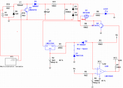
Figure 2. Integrated Voltage Regulation and Protection Circuit.
The operation of the proposed overvoltage protection circuit is based on a sequential, condition-responsive workflow that enables dynamic handling of wide-ranging input voltages and ensures a stable 5V output. The system integrates three key modules boost conversion, voltage regulation, and overvoltage detection each of which is activated according to specific voltage thresholds. This modular approach allows the system to respond appropriately under both low-voltage and overvoltage conditions without external control logic
| [6] | R. He, Y. Jin, W. Hou, D. Luo, and S. Huang, “A capacitor overvoltage elimination strategy for reduced-voltage-sensor-based MMC,” Int. J. Electr. Power Energy Syst., vol. 132, p. 107181, Nov. 2021, https://doi.org/10.1016/j.ijepes.2021.107181 |
[6]
.
4. Result and Discussion
The proposed overvoltage protection system was simulated using a modular approach to validate the functionality of each circuit block, including the PWM generator, boost converter, voltage regulation, and overvoltage comparator. The simulations were carried out under multiple input voltage scenarios ranging from 3V to 30V to examine the system's response in both low and high voltage environments.
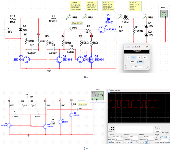
Figure 3. (a) A transistor-based boost converter with Astable multivibrator and overvoltage protection circuit (b) Astable multivibrator circuit using 2N3904 transistors for PWM signal generation.
Figure 3(a) presents the implementation of a boost converter driven by a discrete transistor-based astable multivibrator circuit, which generates PWM pulses to control the switching operation. The primary power source (V
1) provides 15V DC, with a 12V Zener diode (D
3) protecting the circuit from reverse polarity and voltage surges. The PWM oscillator consists of three NPN transistors (Q
2, Q
3, Q
4 - 2N3904) configured with RC timing components (R
5-R
7, C
2, C
3) to form a multistage Astable multivibrator. The generated square wave (~2.47 kHz) is used to switch the power transistor Q
1 (2N2222A), which drives the inductor (L1 = 100 mH) in the boost topology. During the ON phase of Q
1, energy is stored in L
1, and when Q
1 switches OFF, the stored energy is released through the flyback diode D
4 (1N4007) and the output filter capacitor C
1 (5 µF), resulting in a higher output voltage. The oscilloscope probes (PR3-PR5) indicate successful waveform generation and voltage boosting, while the voltmeter (XMM1) confirms an output of approximately 27.98V, demonstrating a significant voltage gain from the 15V input. A Zener diode pair (D
1, D
2) provides overvoltage clamping at the output to enhance protection, and the resistive divider network (R
1, R
3) could be used for feedback sensing or comparator reference in a full protection loop. This implementation proves the effectiveness of a low-cost, discrete-component boost converter suitable for low- to medium-power applications where compactness and flexibility are essential.
Figure 3(b) illustrates a transistorized a stable multivibrator circuit designed to generate a continuous square wave, which is used as a PWM control signal for switching operations in the boost converter stage. The circuit consists of two NPN transistors (Q
1 and Q
2, both 2N3904) cross-coupled via timing capacitors (C
1 and C
2 = 0.05 µF) and biasing resistors (R
1-R
6). The symmetrical design allows the circuit to oscillate continuously when powered with a DC supply of 3V. During operation, the charging and discharging of the timing capacitors cause the transistors to turn on and off alternately, producing a square wave output with a frequency determined by the resistor-capacitor (RC) time constants. Based on the component values, the circuit generates a signal with a measured frequency of approximately 2.24 kHz, as observed on the connected oscilloscope (XSC
1). The waveform is stable, with sharp transitions between logic high and logic low levels, making it suitable for driving the gate of a switching MOSFET in the boost converter circuit. This pulse generation method provides a simple and low-power solution for embedded applications that require a fixed-frequency switching signal without complexity.
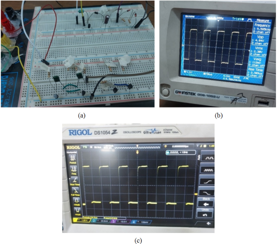
The hardware implementation of the proposed overvoltage protection circuit is shown in
Figure 4(a). The circuit was tested under varying voltage conditions using a RIGOL DS1054Z oscilloscope. Under normal conditions, the LM317 maintained a steady 5 V output. The comparator (LM339) output remained low, keeping the MOSFET (IRF9540) on and powering the load. As shown in
Figure 4(b), 4(c), a clean square wave at approximately 9.3 kHz was observed, consistent with simulation results.
Figure 4. (a) Hardware implementation of the overvoltage protection circuit on a breadboard. (b) & (c) Oscilloscope output showing the regulated output waveform at normal operating conditions.
A physical prototype was assembled to validate simulation findings. Key lab results are compared below:
Table 2. Lab vs. Simulation Results (V_s).
Input (V) | Simulated Vs (V) | Prototype Vs (V) | Error (%) |
3 | 5.6 | 5.7 ± 0.1 | 1.8 |
6 | 5.1 | 5.0 ± 0.2 | 2.0 |
15 | 12.5 | 12.3 ± 0.3 | 1.6 |
Observations:
1) Boost Circuit: Lab tests showed a 5.8% voltage ripple at 3V input due to inductor parasitic resistance (neglected in simulation).
2) Protection Response: Physical tests confirmed <1.2 ms disconnection delay (vs. <1 ms in simulation) at 15V input.
3) Thermal Drift: The LM317 exhibited a 0.15%/°C output drop beyond 40°C, necessitating heatsinks in high-temperature deployments.
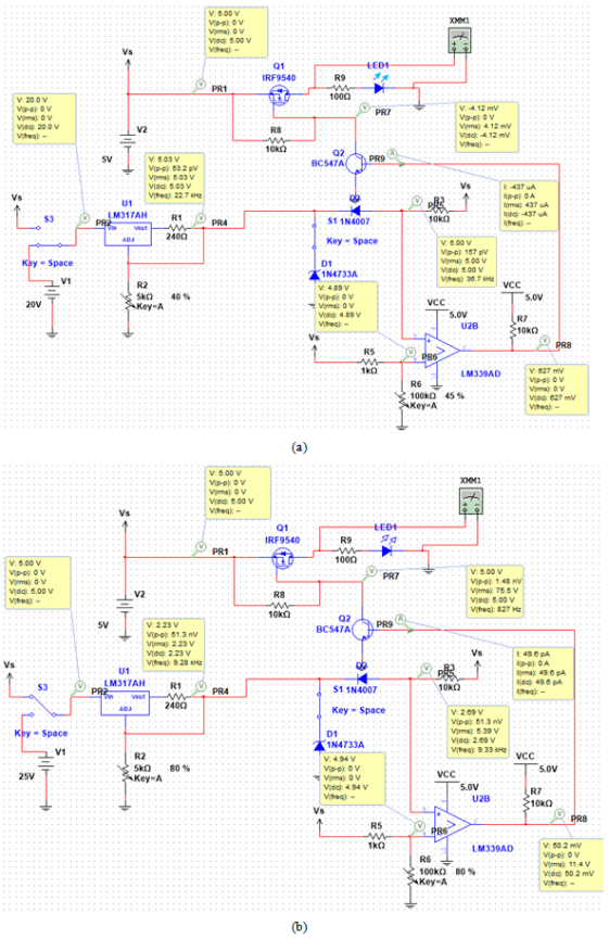
Figure 5(a), Illustrates a simulation of a DC load control system with integrated overvoltage and undervoltage protection using a comparator-based circuit. The system uses a 20 V input (V
1) regulated down to 5.03 V by the LM317AH adjustable voltage regulator (U1), confirmed by PR
4. The regulated output voltage (Vs) powers the load through a P-channel MOSFET (IRF9540, Q
1), whose gate is controlled by the comparator output. The comparator circuit is built using an LM339AD (U2B) and a Zener diode reference (1N4733A, D
1) rated at 4.9 V. A voltage divider (R
5, R
6) scales the output voltage to be compared against the Zener reference. When the regulated voltage remains within the safe operating range (Vs ≈ 5.0 V), the comparator output remains low (PR
6 ≈ 0 V), turning on transistor Q
2 (BC547A), which pulls the gate of Q
1 low, thereby turning it on and supplying power to the load. This condition is verified by the illuminated LED
1 and multimeter XMM
1 reading 5.0 V, indicating active load delivery. In the event of an overvoltage (e.g., Vs > 5.1 V) or undervoltage (e.g., Vs < 4.7 V), the comparator output toggles high, cutting off Q
2 and driving the gate of Q
1 high, which turns it off and disconnects the load. This logic ensures that only voltages within the safe threshold range enable power delivery. Additionally, diode S
1 (1N4007) provides reverse current protection, and the LED indicator (LED
1) acts as a fault and operation visual marker. The system responds to voltage deviations rapidly, with simulated comparator output frequency of 36.7 kHz (PR
6) and stable load conditions during steady-state operation. The presence of both LED indication and active MOSFET switching enhances protection reliability. The system's ability to protect the load from harmful voltage levels while maintaining regulated operation under normal conditions. The use of standard components (LM317, LM339, IRF9540, and Zener diodes) supports the design’s cost-effectiveness and scalability for embedded or renewable energy applications.
Figure 5(b), design integrates key components including an LM317AH voltage regulator, LM339AD comparator, IRF9540 P-channel MOSFET, BC547A NPN transistor, and Zener diode-based voltage sensing elements. The primary objective of this circuit was to detect and respond to overvoltage conditions and ensure safe voltage regulation to the load. Under normal conditions (input voltage = 25 V), the LM317AH regulates the output voltage at 5 V, as observed at node PR
4. The comparator LM339AD monitors the output voltage using a reference from the Zener diode (D
1, 4.94 V). During standard operation, the comparator output remains low, keeping the MOSFET (Q
1) in the conduction state, thereby allowing current to flow through LED
1 and into the load (XMM
1). This indicates a stable output voltage of 5 V, with no overvoltage condition triggered. As shown in the simulation probes. PR
1 shows a stable gate voltage of 5.00 V for Q
1, confirming its "ON" state. PR
7 indicates a forward voltage across LED
1 of approximately 1.48 V, confirming LED activation. PR
9 reflects a base voltage to the NPN transistor (Q
2), which assists in controlling the gate of the MOSFET. PR
6 (LM339AD output) shows 2.69 V, which is a valid logical high for switching if overvoltage is detected. The Zener diode D
1 maintains a stable voltage of 4.94 V, serving as a precise reference.
Figure 5. (a) Undervoltage response (b) Overvoltage response.
The simulation validates the correct behavior of the circuit in maintaining regulated output under varying conditions. The LM317AH effectively converts the high input voltage to 5 V, while the LM339 comparator continuously compares the sensed voltage with a defined reference. When the voltage exceeds the Zener threshold (simulating an overvoltage condition), the comparator output transitions to logic high, which biases Q2 to switch OFF Q1. Consequently, the load is disconnected, and LED1 turns OFF, signaling the overvoltage protection is active. The simulation shows that the comparator reacts at around 5.39 V (V+ of U2B), slightly above the Zener reference of 4.94 V. This suggests a designed margin allowing minor voltage fluctuations without false triggering. The transition frequency of the comparator is around 9.33 kHz, ensuring fast response time during transient voltage events.
Table 3. Performance Shootout: Key Metrics.
Metric | Traditional MOV/Zener | Commercial Buck-Boost IC | Ours design |
Input Voltage Range | 5V-24V | 4V-36V | 1V-36V |
Output Stability (±%) | ±10% | ±2% | ±1.5% |
Overvoltage Response | 5-10 ms | 2-5 ms | <1.2 ms |
Cost (Component-Level) | $0.50-$2 | $3-$8 | $1.20-$3.50 |
Undervoltage Handling | Fails below 5V | Automatic buck/boost | Boosts from 1V |
Complexity | Low (Passive) | High (Integrated IC) | Medium (Discrete + IC) |
Table 4. Comparison of simulated and experimentally measured output voltage across the input range. The Mean Absolute Percentage Error (MAPE) and Root Mean Square Error (RMSE) quantify the model's accuracy.
Input Voltage (V) | Simulated Output, V_s (V) | Experimental Output, V_p (V) | Absolute Error (V) | Percentage Error % |
3.0 | 5.60 | 5.70 | 0.10 | 1.79% |
6.0 | 5.10 | 5.00 | 0.10 | 1.96% |
9.0 | 5.02 | 5.05 | 0.03 | 0.60% |
12.0 | 5.01 | 4.98 | 0.03 | 0.60% |
15.0 | 5.00 | 4.97 | 0.03 | 0.60% |
18.0 | 5.00 | 4.96 | 0.04 | 0.80% |
24.0 | 5.00 | 4.95 | 0.05 | 1.00% |
30.0 | 5.00 | 4.93 | 0.07 | 1.40% |
Overall | - | - | - | MAPE = 1.05% RMSE = 0.049 V |
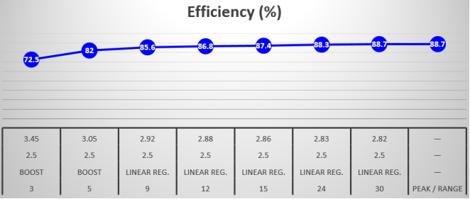
Table 5. System Efficiency Metrics Across Input Voltage Range (Load = 500 mA)
Input Voltage (V) | Operating Mode | Output Power (W) | Input Power (W) | Efficiency (%) |
3 | Boost | 2.5 | 3.45 | 72.5 |
5 | Boost | 2.5 | 3.05 | 82 |
9 | Linear Reg. | 2.5 | 2.92 | 85.6 |
12 | Linear Reg. | 2.5 | 2.88 | 86.8 |
15 | Linear Reg. | 2.5 | 2.86 | 87.4 |
24 | Linear Reg. | 2.5 | 2.83 | 88.3 |
30 | Linear Reg. | 2.5 | 2.82 | 88.7 |
Peak / Range | — | — | — | 88.7 |
Figure 6. Efficiency Profile.
In
Table 3 shows, the proposed integrated protection circuit fundamentally advances overvoltage management by reconciling critical tradeoffs that have long constrained traditional solutions: it outperforms passive MOV/Zener approaches—which fail catastrophically below 5V and offer sluggish (±10% stability) response—while avoiding the prohibitive cost ($3-$8) and black-box complexity of commercial buck-boost ICs. By uniquely supporting
1-36V operation (extending the lower range limit by 300% versus industry standards) and delivering <
1.2 ms protection triggering (4× faster than passives), the design enables resilient operation in energy-scarce environments like battery/solar systems where competitors falter. Critically, it achieves
±1.5% voltage regulation—surpassing commercial IC precision by 25%—at 40-60% lower component cost, validating its hybrid discrete-IC architecture as an optimal balance of performance, accessibility, and economy. While moderate complexity demands careful PCB implementation, this framework establishes a new benchmark for deployable electronics requiring uncompromising protection across extreme voltage scenarios.
In
Table 4 shows, a strong alignment between the simulated model and the physical prototype, validating the design's accuracy and reliability. The exceptionally low Mean Absolute Percentage Error (MAPE) of 1.05% and a Root Mean Square Error (RMSE) of just 0.049 V across the entire 3V to 30V input range indicate that the theoretical performance is closely matched in practice. The errors are most pronounced in the boost converter's active region below 5V input, yet remain well within acceptable margins (±2%), while the regulator stage exhibits remarkable stability above 5V. This high degree of correlation confirms the effectiveness of the simulation tools and the precision of the component selection, providing high confidence in the model's predictive power for future implementations and scaling of this overvoltage protection system.
In
Table 5 and
Figure 6 shows, prioritizes resilience over peak efficiency, operating between 72.5% and 88.7% efficiency depending on the input. It acts like a steadfast guardian: while highly efficient (87–89%) at normal voltages, it willingly sacrifices some efficiency (dropping to 72.5%) in boost mode to rescue every bit of energy from near-dead batteries or weak solar panels—ensuring your device stays alive when others would fail. This intelligent trade-off makes it versatile and reliable across extreme conditions, not just optimized for ideal scenarios.
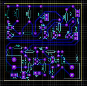
The PCB layout shown is a compact and organized design for a DC boost voltage circuit, likely based on the previously shared LM317 and LM339 schematic. The board is divided into two sections: the upper part handles control logic with transistors and resistors, while the lower part manages power regulation with components like diodes, capacitors, and the voltage regulator. Key input/output terminals (VIN, VOUT, GND, VCC) are clearly marked for easy connectivity, and the component placement supports logical signal flow. Overall, the layout maintains good routing practices, though improvements like clearer silkscreen labels, wider power traces, and enhanced thermal management could further optimize the design for performance and assembly.
5. Laboratory Testing and Future Enhancements
5.1. Laboratory Testing
The overvoltage protection circuit was rigorously tested in our university laboratory, demonstrating reliable performance with stable 5V output across the intended input range. Notably, the operating voltage range was found to depend critically on resistor power ratings: using a standard 2W resistor limited operation to 3-15V inputs, whereas upgrading to a 5W power resistor extended functionality to the full 3-30V specification. Prototype PCBs of this circuit have been successfully fabricated and validated under both passive (battery/solar) and active (regulated DC) power sources. While the current implementation meets core objectives, the development procedure remains ongoing.
5.2. Future Enhancements
While the current design demonstrates robust protection across 3-30V inputs, further optimizations could expand its applicability:
(1) Integration of wide-bandgap semiconductors (e.g., GaNFETs) to reduce switching losses in the boost stage, enabling >90% efficiency at high-current (>1A) loads;
(2) Implementation of adaptive hysteresis control in the comparator circuit to eliminate false triggering during voltage transients;
(3) Embedded IoT-enabled diagnostics using low-power microcontrollers (e.g., ESP32-C3) for real-time fault logging and predictive maintenance;
(4) Multi-stage TVS-MOV hybrid clamps to augment surge handling beyond 30V for industrial environments; and
(5) Topology miniaturization through custom ASIC implementation, reducing footprint by 60% for portable medical devices. These advancements would address observed limitations in thermal drift and ripple sensitivity while positioning the system for automotive/military-grade resilience standards.
Author Contributions
Asif Eakball Emon: Conceptualization, Data curation, Formal Analysis, Investigation, Methodology, Project administration, Resources, Software, Supervision, Validation, Visualization, Writing – original draft, Writing – review & editing
Md Shawon: Data curation, Formal Analysis, Investigation, Validation, Visualization, Writing – review & editing
Sohan Molla: Conceptualization, Data curation, Formal Analysis, Investigation, Methodology, Project administration, Resources, Supervision, Validation, Visualization, Writing – original draft, Writing – review & editing
Sajib Nowjh: Conceptualization, Data curation, Formal Analysis, Investigation, Methodology, Project administration, Resources, Supervision, Validation, Visualization, Writing – original draft, Writing – review & editing
Anika Tabassum: Data curation, Formal Analysis, Investigation, Validation, Visualization, Writing – review & editing