Department of Electrical & Electronic Engineering, Faculty of Engineering and Applied Sciences, Bangladesh University of Business & Technology (BUBT), Dhaka, Bangladesh
Department of Electrical & Electronic Engineering, Faculty of Engineering and Applied Sciences, Bangladesh University of Business & Technology (BUBT), Dhaka, Bangladesh
Contributor Roles: Conceptualization, Data curation, Formal Analysis, Investigation, Methodology, Project administration, Resources, Writing – original draft
Department of Electrical & Electronic Engineering, Faculty of Engineering and Applied Sciences, Bangladesh University of Business & Technology (BUBT), Dhaka, Bangladesh
Contributor Roles: Conceptualization, Data curation, Formal Analysis, Funding acquisition, Resources, Visualization, Writing – original draft, Writing – review & editing
Department of Electrical & Electronic Engineering, Faculty of Engineering and Applied Sciences, Bangladesh University of Business & Technology (BUBT), Dhaka, Bangladesh
Department of Electrical & Electronic Engineering, Faculty of Engineering and Applied Sciences, Bangladesh University of Business & Technology (BUBT), Dhaka, Bangladesh
Department of Electrical & Electronic Engineering, Faculty of Engineering and Applied Sciences, Bangladesh University of Business & Technology (BUBT), Dhaka, Bangladesh
The increasing demand for efficient power regulation in embedded systems, renewable energy, and portable electronics has elevated the importance of DC-DC converters in modern power electronics. Among them, the buck converter a type of step-down converter is widely favored due to its high efficiency, compactness, and suitability for low-voltage applications. This study was undertaken to explore the design, simulation, and hardware implementation of a buck converter capable of stepping down a 12 V DC input to output levels of 3 V, 6 V, and 9 V based on duty cycles of 25%, 50%, and 75%, respectively. The objective was to validate theoretical predictions using both simulation and physical testing. The circuit design incorporated essential power electronic components such as IRF9530 MOSFETs, IR2110 driver IC, inductors, capacitors, and freewheeling diodes, assembled on a Vero board for prototype development. Proteus simulation results closely followed expected voltage levels, while hardware testing showed minor deviations due to non-idealities like component tolerances, switching losses, and thermal effects. The comparison between theoretical, simulated, and measured outputs confirmed the operational integrity and efficiency of the design. In addition to the technical focus, this work considers safety measures, ethical responsibility, and environmental impact ensuring the converter's alignment with modern sustainable engineering practices. This project not only demonstrates the functional reliability of buck converters in real-world scenarios but also contributes to students’ hands-on learning and fosters innovation in scalable energy systems.
This is an Open Access article, distributed under the terms of the Creative Commons Attribution 4.0 International License (http://creativecommons.org/licenses/by/4.0/), which permits unrestricted use, distribution and reproduction in any medium or format, provided the original work is properly cited.
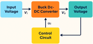
The buck converter, also known as a step-down converter, is a fundamental topology in switched-mode power supply (SMPS) systems, widely recognized for its ability to efficiently reduce a higher input voltage to a lower output voltage. Due to its relatively simple design and high efficiency, the buck converter is extensively applied in a variety of domains including embedded systems, industrial automation, telecommunications, and consumer electronics
[1]
Md. Fahim Hasan Khan, Sadman Sakib, Md. Ashiqur Rahman, and Md. Zamilur Reza, “DC-DC and AC-DC Zeta and Buck Converter Design and Analysis for High Efficiency Application,” 2017,
. Its core operating principle revolves around the rapid switching of a semiconductor device, typically a MOSFET, and the regulated transfer of energy through an inductor-capacitor (LC) network. This project aims to design, simulate, and implement a functional buck converter capable of stepping down a DC voltage input of 12 V to lower levels determined by varying the duty cycle of a pulse-width modulation (PWM) signal
[2]
B. A. Altug, A. Kababiyik, E. Dincol, and C. Batunlu, “Buck Converter with Optocoupler Based Switching,” in 2021 8th International Conference on Electrical and Electronics Engineering (ICEEE), Antalya, Turkey: IEEE, Apr. 2021, pp. 184-190.
. Theoretical calculations were validated through both simulation and hardware implementation to assess converter performance across different operating conditions. Specifically, output voltages were measured for duty cycles of 25%, 50%, and 75%, confirming expected step-down behavior
[3]
“Digital control strategies of DC-DC converters in automotive hybrid powertrains,” in Modeling, Operation, and Analysis of DC Grids, Elsevier, 2021, pp. 245-287.
The simulation and hardware results demonstrate the converter’s functionality, revealing minor deviations in practical implementation due to component non-idealities, switching losses, and thermal effects. These discrepancies are analyzed and compared with theoretical predictions, providing insights into practical design considerations necessary for optimizing converter efficiency and performance. The outcome of this study underscores the viability of the buck converter as a reliable solution for voltage regulation tasks within electronic systems
[4]
H. Sucu, T. Göktaş, and M. Arkan, “Design, Simulation and Application of Buck Converter with Digital PI Controller,” Balk. J. Electr. Comput. Eng., vol. 9, no. 2, pp. 106-113, Apr. 2021,
The buck converter, a type of DC-DC step-down power supply, has been extensively researched due to its widespread utility in voltage regulation for various electronics and power systems. Originating from the field of switched-mode power supply (SMPS) design, buck converters continue to play a critical role in both analog and digital power regulation systems. According to Erickson and Maksimović (2001), buck converters operate on the principle of storing and transferring energy through inductive and capacitive elements while modulating the switching duty cycle to regulate output voltage. Their efficiency is typically high often above 85% and, faster switching, and lower conduction losses. These wide-bandgap semiconductors allow higher switching frequencies, reducing the size of passive components and improving transient response. Academic works such as those by Wu et al. (2022) and Huang et al. (2023) have also explored multi-phase buck converters, which distribute current across multiple phases to improve efficiency, thermal management, and current handling in high-load scenarios. Furthermore, integrated magnetic components and PCB-embedded inductors have been introduced to enhance space efficiency in power modules
[5]
M. Abolghasemi, I. Soltani, M. Shivaie, and H. Vahedi, “Recent advances of step-up multi-stage DC-DC converters: A review on classifications, structures and grid applications,” Energy Rep., vol. 13, pp. 3050-3081, Jun. 2025,
. Collectively, these advancements reinforce the importance of comprehensive modeling, precise control, and efficient hardware design to achieve optimal performance in buck converter systems, particularly in mission-critical and space-constrained occasionally exceeding 95% due to minimal energy dissipation in ideal conditions. This makes them especially valuable in low-power, high-efficiency applications such as portable electronics and embedded systems
[6]
“Current Programmed Control,” in Fundamentals of Power Electronics, Boston, MA: Springer US, 2001, pp. 439-487.
. Simulation-based studies, such as those using Spice or MATLAB/Simulink environments, have validated the relationship between duty cycle and output voltage (Vo = Vin × D), where Vin is the input voltage and D is the duty cycle. Practical work often confirms this behavior under controlled conditions. However, discrepancies between simulation and experimental results arise due to non-ideal characteristics of components, including switching losses, parasitic capacitance, and electromagnetic interference
[3]
“Digital control strategies of DC-DC converters in automotive hybrid powertrains,” in Modeling, Operation, and Analysis of DC Grids, Elsevier, 2021, pp. 245-287.
. Describes reduced output impedance in PWM buck converters using genetic algorithms for control optimization
[7]
F. Asadi̇, “Reduction of Output Impedance of Buck Converter with Genetic Algorithm,” Balk. J. Electr. Comput. Eng., vol. 10, no. 3, pp. 317-322, Jul. 2022,
. Recent advancements have introduced high-frequency switching and improved control strategies, such as hysteretic and current-mode control, which have further enhanced transient response and reduced output ripple
[8]
Jingquan Chen, D. Maksimovic, and R. W. Erickson, “Analysis and design of a low-stress buck-boost converter in universal-input PFC applications,” IEEE Trans. Power Electron., vol. 21, no. 2, pp. 320-329, Mar. 2006,
. These improvements enable finer output regulation and system stability under varying load conditions. In practical implementation, researchers have emphasized the importance of accurate component selection and thermal management. For instance, inductor core material and MOSFET switching speed directly affect efficiency and heat dissipation. Moreover, discrepancies observed between simulation and hardware are often attributed to model inaccuracies, component tolerances, and layout-induced parasitic, aligning with findings from prior studies
[9]
C. Jiang, C. Chai, Y. Yang, Y. Liu, and Y. Yang, “An IAOT controlled current-mode buck converter with RC-based inductor current sensor,” IEICE Electron. Express, vol. 17, no. 4, pp. 20190757-20190757, 2020,
. A Novel Winding-Coupled Buck Converter introduces a high frequency, high step-down topology achieving over 80% efficiency at 2 MHz switching
[10]
K. Yao, Y. Qiu, M. Xu, and F. C. Lee, “A Novel Winding-Coupled Buck Converter for High-Frequency, High-Step-Down DC-DC Conversion,” IEEE Trans. Power Electron., vol. 20, no. 5, pp. 1017-1024, Sep. 2005,
. Overall, existing research supports the robustness of buck converter theory and affirms the viability of simulation tools for predictive analysis. Nonetheless, careful attention to design limitations and non-ideal parameters remains essential for achieving reliable, high-performance converter systems. In recent years, the evolution of buck converter technologies has been driven by the growing demand for compact, reliable, and energy-efficient power solutions across a wide range of industries. Studies such as those by Rashid (2017) and Mohan et al. (2020) have underscored the buck converter’s critical role in modern power architecture, especially in battery-powered devices, Internet of Things (IoT) systems, and renewable energy applications. These studies highlight improvements in converter topologies that enable dynamic voltage scaling, better thermal distribution, and high power density, which are essential for today’s miniaturized electronics
[11]
R. Singh, V. Kurukuru, and M. Khan, “Advanced Power Converters and Learning in Diverse Robotic Innovation: A Review,” Energies, vol. 16, no. 20, p. 7156, Oct. 2023,
. Modern buck converters increasingly leverage soft-switching techniques such as Zero Voltage Switching (ZVS) and Zero Current Switching (ZCS) to minimize switching losses and electromagnetic interference (EMI). These methods significantly improve converter efficiency, especially in high-frequency operations. Recent literature also explores digital control strategies, including adaptive and predictive control algorithms implemented through microcontrollers or digital signal processors (DSPs), to enhance regulation precision under dynamic load conditions. Moreover, Gallium Nitride (GaN) and Silicon Carbide (SiC) based devices are becoming popular replacements for traditional silicon MOSFETs due to their superior thermal performance applications.
3. Methodology
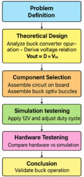
The methodology of this study focuses on the design, simulation, and hardware implementation of a buck converter, aimed at demonstrating effective DC-DC voltage step-down functionality based on varying duty cycles. The approach is structured into three main phases: theoretical modeling, simulation, and hardware realization
[12]
P. Alavi, E. Babaei, P. Mohseni, and V. Marzang, “Study and analysis of a DC-DC soft‐switched buck converter,” IET Power Electron., vol. 13, no. 7, pp. 1456-1465, May 2020,
Figure 2 the flowchart illustrates the complete development process of a buck converter, beginning with the clear definition of the problem designing a circuit to step down DC voltage using a buck converter. It proceeds to the theoretical design phase, where the operating principle is analyzed, and the key voltage relation is derived to guide the expected output behavior. Following this, essential components such as MOSFETs, diodes, inductors, capacitors, and the IR2110 driver are selected and organized for circuit assembly
[13]
“Computational Investigation of Cs2BiAgI6 for Perovskite Solar Cell Applications Using SCAPS-1D,” J. Sustain. Dev. Innov., vol. 2, no. 2, 2025,
. The simulation testing phase involves assembling the circuit virtually or on a test board, applying a constant 12 V input, and varying the duty cycle to observe the corresponding changes in output voltage
[14]
S. Molla, M. Shawon, M. Nawaj, and A. Emon, “Analysis of Aging Effect and Cell Balancing Problem of Lithium-Ion Battery,” J. Electr. Electron. Eng., vol. 13, no. 2, pp. 92-107, Mar. 2025,
After validating the theoretical performance through simulation, hardware testing is conducted to replicate the conditions in a real-world setup, where the measured output voltages are compared with simulated results to analyze consistency and identify possible deviations due to non-idealities like component tolerances and switching losses. Finally, the project concludes by confirming the buck converter’s step-down functionality, ensuring that the system performs efficiently and reliably in practice as it was intended in theory and simulation
[2]
B. A. Altug, A. Kababiyik, E. Dincol, and C. Batunlu, “Buck Converter with Optocoupler Based Switching,” in 2021 8th International Conference on Electrical and Electronics Engineering (ICEEE), Antalya, Turkey: IEEE, Apr. 2021, pp. 184-190.
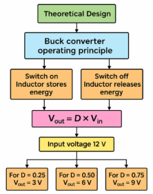
The buck converter is a type of DC-DC step-down converter that operates by periodically switching a power transistor to regulate the voltage supplied to a load. Its fundamental operating principle is based on the controlled transfer of energy from the input to the output through an inductor and a switching element. The converter reduces the input voltage by modulating the duty cycle of the switch, making it suitable for applications that require efficient voltage regulation. When the switch (typically a MOSFET) is turned ON, the inductor is directly connected to the input voltage source
[15]
D. G. Aller, D. G. Lamar, J. R. García-Mere, M. Arias, J. Rodriguez, and J. Sebastian, “Performance Evaluation of the Two-Input Buck Converter as a Visible Light Communication High-Brightness LED Driver Based on Split Power,” Sensors, vol. 24, no. 19, p. 6392, Oct. 2024,
. During this phase, current flows through the inductor and energy is stored in its magnetic field. Simultaneously, the diode becomes reverse-biased, preventing current from flowing backward. When the switch is turned OFF, the inductor maintains current flow by releasing stored energy. The diode becomes forward-biased, allowing current to continue flowing through the inductor to the output capacitor and load. The output capacitor helps maintain a steady voltage by smoothing out voltage ripples caused by the switching operation
[16]
S. Masri, N. Mohamad, and M. H. M. Hariri, “Design and development of DC-DC buck converter for photovoltaic application,” in 2012 International Conference on Power Engineering and Renewable Energy (ICPERE), Bali, Indonesia: IEEE, Jul. 2012, pp. 1-5.
Figure 2. Flowchart of Buck Converter Design and Testing Process.
The relationship between the output voltage Vout, the input voltage Vin, and the duty cycle D (defined as the ratio of the ON time to the total switching period) is given by:
Vout=D×Vin(1)
Where, Vout is the average output voltage, Vin is the input supply voltage, D is the duty cycle (0 ≤ D ≤ 1).
For this project, the input voltage was maintained at a constant 12 V. The expected output voltages were calculated using the formula above for varying duty cycles:
[13]
“Computational Investigation of Cs2BiAgI6 for Perovskite Solar Cell Applications Using SCAPS-1D,” J. Sustain. Dev. Innov., vol. 2, no. 2, 2025,
The buck converter utilizes a variety of components to ensure efficient voltage step-down operation. IRF9530 MOSFETs serve as the main switching devices, controlled by the IR2110 driver IC, which ensures proper gate operation. Two 7805 voltage regulators provide a stable 5V supply for control circuits. Capacitors of various ratings (1 µF, 22 µF, 0.1 nF) are used for filtering and noise suppression, driver, while 820 µH inductors store and release energy during switching cycles. Freewheeling diodes (1N4007) maintain current flow when the switch is off, and 220 Ω resistors are used for current limiting and control. Load resistors simulate real-world operating conditions for testing, and the entire circuit is assembled on a Vero board. Banana plugs and sockets serve as connectors for secure and flexible external connections to power sources and measurement tools
[17]
A. Emon, M. Shawon, S. Molla, and M. Nowjh, “Improved Microgrid Controller with Robust Stability, Conjunction with PID Controllers,” J. Electr. Electron. Eng., vol. 13, no. 3, pp. 116-130, May 2025,
Table 1. List of Components Used in the Buck Converter Design.
Component
Specification
Quantity
MOSFET
IRF9530
2
Driver IC
IR2110
1
Voltage Regulator
7805
2
Capacitors
1 µF, 22 µF, 0.1 nF
Various
Inductor
820 µH
5
Diodes
1N4007
10
Resistors
220 Ω
50
Load Resistors
-
2
PCB / Vero Board
-
1
Connectors
Banana plugs/sockets
Various
4. Results
The flowchart visually represents the theoretical design of a buck converter, outlining its fundamental operating principle. It begins with the concept that the converter operates by switching a transistor on and off when the switch is on, the inductor stores energy, and when the switch is off, the inductor releases that energy to the load. The relationship between output voltage and duty cycle is defined by the equation Vout. Vin is fixed at 12V. This theoretical framework predicts specific output voltages based on different duty cycles. The diagram effectively shows how controlling the duty cycle adjusts the output voltage, confirming the step-down behavior fundamental to buck converter operation.
Figure 3. Theoretical Operation of a Buck Converter.
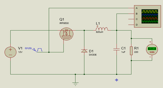
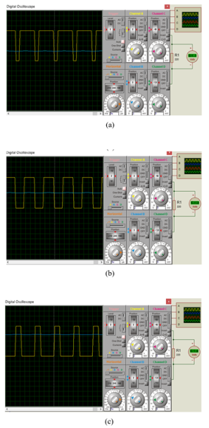
4.1. Simulation
Simulation of the buck converter circuit was performed using proteus software a standard power electronics simulation tool. The simulation included all essential passive and active components a switching MOSFET (IRF9530), an inductor, a freewheeling diode (1N4007), and output filter capacitors. The duty cycles were varied systematically (25%, 50%, 75%) to observe and verify the expected output voltage levels.
Figure 4 the circuit uses a P-channel MOSFET (IRF9530) labeled Q1 as the main switching element. The input voltage source (V1) supplies 12V, and a PWM signal is applied to the gate of Q1 to control its switching operation. When the MOSFET turns ON, current flows through the inductor (L1, 820 µH), storing energy in its magnetic field. When the MOSFET turns OFF, the freewheeling diode (D1) becomes forward-biased, and the inductor releases its stored energy through the capacitor (C1, 1 µF) and load resistor (R1, 220 Ω). The capacitor smooths out voltage ripples to maintain a stable DC output.
4.2. Simulation Results
The buck converter circuit was simulated using standard circuit simulation software. The simulations were conducted for three distinct duty cycles, 25%, 50%, and 75%, with an input voltage of 12V maintained consistently throughout all tests.
Figure 5. Simulation Output (a) 25% duty cycle average output voltage and graph (b) 50% duty cycle average output voltage and graph (c) 75% duty cycle average output voltage and graph.
The simulated output voltages were as follows:
Table 2. Comparison of Theoretical, Simulated, and Hardware Output Voltages at Different Duty Cycles.
Duty Cycle
Theoretical Output (V)
Simulated Output (V)
Simulation Output (V)
25%
3.00
3.06
~3.00
50%
6.00
5.91
~6.00
75%
9.00
8.67
~9.00
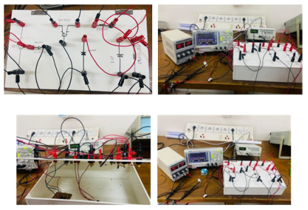
4.3. Hardware Implementation
The hardware prototype was constructed on a Vero board using commercially available discrete components as per the simulation model.
Figure 6. Hardware base buck converter circuit diagram (setup).
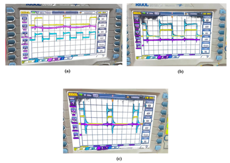
4.4. Hardware Result
Connections were securely soldered and enclosed in a protective casing. Oscilloscope readings were obtained at the output terminals to record real-time voltage under various duty cycle settings.
Table 3. Comparison of Theoretical, Simulated, and Hardware Output Voltages at Different Duty Cycles.
Duty Cycle
Theoretical Output (V)
Simulated Output (V)
Hardware Output (V)
25%
3.00
2.96
~3.00
50%
6.00
5.60
~6.00
75%
9.00
8.37
~9.00
4.5. Expected Result
Based on the theoretical operation of a buck converter, the output voltage is directly proportional to the product of the duty cycle and the input voltage. For a fixed input of 12V, the expected output voltages under ideal conditions are as follows: 3V for a 25% duty cycle, 6V for a 50% duty cycle, and 9V for a 75% duty cycle. These values assume ideal components with no losses, such as zero voltage drop across the diode, no internal resistance in the inductor, and perfect switching behavior of the MOSFET. These outputs serve as reference benchmarks for comparison with both simulation and hardware testing results.
For 25% duty cycle,
Average output voltage Vo= Vs ×D =12×0.25 =3V [D =25% and Vs =12V]
For 25% duty cycle,
Average output voltage Vo= Vs ×D =12×0.50 =6 V [D =50% and Vs =12 V]
For 25% duty cycle,
Average output voltage Vo= Vs ×D =12×0.75 =9 V [D =75% and Vs =12 V]
Measured average output voltages under the corresponding duty cycles were. Approximately 3V at 25% duty cycle, approximately 6V at 50% duty cycle, approximately 9V at 75% duty cycle. Although there were minor deviations from the ideal values, these were attributed to non-ideal behavior in physical components, switching losses, and tolerances in passive elements.
5. Conclusions
This research presented a comprehensive approach to the design, simulation, and hardware implementation of a buck converter aimed at efficient DC voltage regulation. The converter was developed to step down a constant 12V input to output levels of approximately 3V, 6V, and 9V, corresponding to duty cycles of 25%, 50%, and 75%, respectively. Through theoretical modeling, circuit simulation using Proteus, and real-world hardware testing, the study validated the expected operational characteristics of the converter. Simulation results demonstrated close agreement with theoretical calculations, while hardware testing revealed minor deviations primarily attributed to non-idealities in physical components, switching losses, and thermal effects. Nonetheless, the converter consistently exhibited stable and predictable voltage regulation behavior, confirming the accuracy of the design and its suitability for practical applications. Beyond the technical achievements, the study incorporated considerations of safety, ethical responsibility, and environmental impact, aligning with best practices in sustainable engineering. The work also provided a valuable educational platform, enhancing practical skills and conceptual understanding among students engaged in the project. The findings affirm the effectiveness of the buck converter for use in embedded systems, renewable energy systems, and consumer electronics requiring reliable step-down voltage conversion. The results contribute to the broader field of power electronics by offering a validated reference design and implementation methodology. Future research may focus on incorporating advanced control strategies, higher switching frequencies, and wide-bandgap semiconductor technologies to further improve performance, efficiency, and integration in compact power management solutions.
Abbreviations
DC
Direct Current
AC
Alternating Current
PWM
Pulse Width Modulation
SMPS
Switched-Mode Power Supply
MOSFET
Metal-Oxide-Semiconductor Field-Effect Transistor
IC
Integrated Circuit
DSP
Digital Signal Processor
EMI
Electromagnetic Interference
ZVS
Zero Voltage Switching
ZCS
Zero Current Switching
GaN
Gallium Nitride
SiC
Silicon Carbide
Vo
Output Voltage
Vin
Input Voltage
IoT
Internet of Things
PCB
Printed Circuit Board
IR
International Rectifier (used in IC and MOSFET Model Names like IR2110, IRF9530)
Md. Fahim Hasan Khan, Sadman Sakib, Md. Ashiqur Rahman, and Md. Zamilur Reza, “DC-DC and AC-DC Zeta and Buck Converter Design and Analysis for High Efficiency Application,” 2017,
B. A. Altug, A. Kababiyik, E. Dincol, and C. Batunlu, “Buck Converter with Optocoupler Based Switching,” in 2021 8th International Conference on Electrical and Electronics Engineering (ICEEE), Antalya, Turkey: IEEE, Apr. 2021, pp. 184-190.
“Digital control strategies of DC-DC converters in automotive hybrid powertrains,” in Modeling, Operation, and Analysis of DC Grids, Elsevier, 2021, pp. 245-287.
H. Sucu, T. Göktaş, and M. Arkan, “Design, Simulation and Application of Buck Converter with Digital PI Controller,” Balk. J. Electr. Comput. Eng., vol. 9, no. 2, pp. 106-113, Apr. 2021,
M. Abolghasemi, I. Soltani, M. Shivaie, and H. Vahedi, “Recent advances of step-up multi-stage DC-DC converters: A review on classifications, structures and grid applications,” Energy Rep., vol. 13, pp. 3050-3081, Jun. 2025,
F. Asadi̇, “Reduction of Output Impedance of Buck Converter with Genetic Algorithm,” Balk. J. Electr. Comput. Eng., vol. 10, no. 3, pp. 317-322, Jul. 2022,
Jingquan Chen, D. Maksimovic, and R. W. Erickson, “Analysis and design of a low-stress buck-boost converter in universal-input PFC applications,” IEEE Trans. Power Electron., vol. 21, no. 2, pp. 320-329, Mar. 2006,
C. Jiang, C. Chai, Y. Yang, Y. Liu, and Y. Yang, “An IAOT controlled current-mode buck converter with RC-based inductor current sensor,” IEICE Electron. Express, vol. 17, no. 4, pp. 20190757-20190757, 2020,
K. Yao, Y. Qiu, M. Xu, and F. C. Lee, “A Novel Winding-Coupled Buck Converter for High-Frequency, High-Step-Down DC-DC Conversion,” IEEE Trans. Power Electron., vol. 20, no. 5, pp. 1017-1024, Sep. 2005,
R. Singh, V. Kurukuru, and M. Khan, “Advanced Power Converters and Learning in Diverse Robotic Innovation: A Review,” Energies, vol. 16, no. 20, p. 7156, Oct. 2023,
P. Alavi, E. Babaei, P. Mohseni, and V. Marzang, “Study and analysis of a DC-DC soft‐switched buck converter,” IET Power Electron., vol. 13, no. 7, pp. 1456-1465, May 2020,
S. Molla, M. Shawon, M. Nawaj, and A. Emon, “Analysis of Aging Effect and Cell Balancing Problem of Lithium-Ion Battery,” J. Electr. Electron. Eng., vol. 13, no. 2, pp. 92-107, Mar. 2025,
D. G. Aller, D. G. Lamar, J. R. García-Mere, M. Arias, J. Rodriguez, and J. Sebastian, “Performance Evaluation of the Two-Input Buck Converter as a Visible Light Communication High-Brightness LED Driver Based on Split Power,” Sensors, vol. 24, no. 19, p. 6392, Oct. 2024,
S. Masri, N. Mohamad, and M. H. M. Hariri, “Design and development of DC-DC buck converter for photovoltaic application,” in 2012 International Conference on Power Engineering and Renewable Energy (ICPERE), Bali, Indonesia: IEEE, Jul. 2012, pp. 1-5.
A. Emon, M. Shawon, S. Molla, and M. Nowjh, “Improved Microgrid Controller with Robust Stability, Conjunction with PID Controllers,” J. Electr. Electron. Eng., vol. 13, no. 3, pp. 116-130, May 2025,
Shawon, M., Molla, S., Fatiha, T., Emon, A. E., Sen, U., et al. (2025). Design, Simulation, and Implementation of a Buck Converter for Efficient DC Voltage Regulation. Journal of Electrical and Electronic Engineering, 13(4), 205-213. https://doi.org/10.11648/j.jeee.20251304.15
Shawon, M.; Molla, S.; Fatiha, T.; Emon, A. E.; Sen, U., et al. Design, Simulation, and Implementation of a Buck Converter for Efficient DC Voltage Regulation. J. Electr. Electron. Eng.2025, 13(4), 205-213. doi: 10.11648/j.jeee.20251304.15
Shawon M, Molla S, Fatiha T, Emon AE, Sen U, et al. Design, Simulation, and Implementation of a Buck Converter for Efficient DC Voltage Regulation. J Electr Electron Eng. 2025;13(4):205-213. doi: 10.11648/j.jeee.20251304.15
@article{10.11648/j.jeee.20251304.15,
  author = {Md Shawon and Sohan Molla and Tahrim Fatiha and Asif Eakball Emon and Utsa Sen and Kanij Fatima},
  title = {Design, Simulation, and Implementation of a Buck Converter for Efficient DC Voltage Regulation
},
  journal = {Journal of Electrical and Electronic Engineering},
  volume = {13},
  number = {4},
  pages = {205-213},
  doi = {10.11648/j.jeee.20251304.15},
  url = {https://doi.org/10.11648/j.jeee.20251304.15},
  eprint = {https://article.sciencepublishinggroup.com/pdf/10.11648.j.jeee.20251304.15},
  abstract = {The increasing demand for efficient power regulation in embedded systems, renewable energy, and portable electronics has elevated the importance of DC-DC converters in modern power electronics. Among them, the buck converter a type of step-down converter is widely favored due to its high efficiency, compactness, and suitability for low-voltage applications. This study was undertaken to explore the design, simulation, and hardware implementation of a buck converter capable of stepping down a 12 V DC input to output levels of 3 V, 6 V, and 9 V based on duty cycles of 25%, 50%, and 75%, respectively. The objective was to validate theoretical predictions using both simulation and physical testing. The circuit design incorporated essential power electronic components such as IRF9530 MOSFETs, IR2110 driver IC, inductors, capacitors, and freewheeling diodes, assembled on a Vero board for prototype development. Proteus simulation results closely followed expected voltage levels, while hardware testing showed minor deviations due to non-idealities like component tolerances, switching losses, and thermal effects. The comparison between theoretical, simulated, and measured outputs confirmed the operational integrity and efficiency of the design. In addition to the technical focus, this work considers safety measures, ethical responsibility, and environmental impact ensuring the converter's alignment with modern sustainable engineering practices. This project not only demonstrates the functional reliability of buck converters in real-world scenarios but also contributes to students’ hands-on learning and fosters innovation in scalable energy systems.},
 year = {2025}
}
TY  - JOUR
T1  - Design, Simulation, and Implementation of a Buck Converter for Efficient DC Voltage Regulation

AU  - Md Shawon
AU  - Sohan Molla
AU  - Tahrim Fatiha
AU  - Asif Eakball Emon
AU  - Utsa Sen
AU  - Kanij Fatima
Y1  - 2025/08/16
PY  - 2025
N1  - https://doi.org/10.11648/j.jeee.20251304.15
DO  - 10.11648/j.jeee.20251304.15
T2  - Journal of Electrical and Electronic Engineering
JF  - Journal of Electrical and Electronic Engineering
JO  - Journal of Electrical and Electronic Engineering
SP  - 205
EP  - 213
PB  - Science Publishing Group
SN  - 2329-1605
UR  - https://doi.org/10.11648/j.jeee.20251304.15
AB  - The increasing demand for efficient power regulation in embedded systems, renewable energy, and portable electronics has elevated the importance of DC-DC converters in modern power electronics. Among them, the buck converter a type of step-down converter is widely favored due to its high efficiency, compactness, and suitability for low-voltage applications. This study was undertaken to explore the design, simulation, and hardware implementation of a buck converter capable of stepping down a 12 V DC input to output levels of 3 V, 6 V, and 9 V based on duty cycles of 25%, 50%, and 75%, respectively. The objective was to validate theoretical predictions using both simulation and physical testing. The circuit design incorporated essential power electronic components such as IRF9530 MOSFETs, IR2110 driver IC, inductors, capacitors, and freewheeling diodes, assembled on a Vero board for prototype development. Proteus simulation results closely followed expected voltage levels, while hardware testing showed minor deviations due to non-idealities like component tolerances, switching losses, and thermal effects. The comparison between theoretical, simulated, and measured outputs confirmed the operational integrity and efficiency of the design. In addition to the technical focus, this work considers safety measures, ethical responsibility, and environmental impact ensuring the converter's alignment with modern sustainable engineering practices. This project not only demonstrates the functional reliability of buck converters in real-world scenarios but also contributes to students’ hands-on learning and fosters innovation in scalable energy systems.
VL  - 13
IS  - 4
ER  -
Department of Electrical & Electronic Engineering, Faculty of Engineering and Applied Sciences, Bangladesh University of Business & Technology (BUBT), Dhaka, Bangladesh
Department of Electrical & Electronic Engineering, Faculty of Engineering and Applied Sciences, Bangladesh University of Business & Technology (BUBT), Dhaka, Bangladesh
Department of Electrical & Electronic Engineering, Faculty of Engineering and Applied Sciences, Bangladesh University of Business & Technology (BUBT), Dhaka, Bangladesh
Department of Electrical & Electronic Engineering, Faculty of Engineering and Applied Sciences, Bangladesh University of Business & Technology (BUBT), Dhaka, Bangladesh
Department of Electrical & Electronic Engineering, Faculty of Engineering and Applied Sciences, Bangladesh University of Business & Technology (BUBT), Dhaka, Bangladesh
Department of Electrical & Electronic Engineering, Faculty of Engineering and Applied Sciences, Bangladesh University of Business & Technology (BUBT), Dhaka, Bangladesh
Shawon, M., Molla, S., Fatiha, T., Emon, A. E., Sen, U., et al. (2025). Design, Simulation, and Implementation of a Buck Converter for Efficient DC Voltage Regulation. Journal of Electrical and Electronic Engineering, 13(4), 205-213. https://doi.org/10.11648/j.jeee.20251304.15
Shawon, M.; Molla, S.; Fatiha, T.; Emon, A. E.; Sen, U., et al. Design, Simulation, and Implementation of a Buck Converter for Efficient DC Voltage Regulation. J. Electr. Electron. Eng.2025, 13(4), 205-213. doi: 10.11648/j.jeee.20251304.15
Shawon M, Molla S, Fatiha T, Emon AE, Sen U, et al. Design, Simulation, and Implementation of a Buck Converter for Efficient DC Voltage Regulation. J Electr Electron Eng. 2025;13(4):205-213. doi: 10.11648/j.jeee.20251304.15
@article{10.11648/j.jeee.20251304.15,
  author = {Md Shawon and Sohan Molla and Tahrim Fatiha and Asif Eakball Emon and Utsa Sen and Kanij Fatima},
  title = {Design, Simulation, and Implementation of a Buck Converter for Efficient DC Voltage Regulation
},
  journal = {Journal of Electrical and Electronic Engineering},
  volume = {13},
  number = {4},
  pages = {205-213},
  doi = {10.11648/j.jeee.20251304.15},
  url = {https://doi.org/10.11648/j.jeee.20251304.15},
  eprint = {https://article.sciencepublishinggroup.com/pdf/10.11648.j.jeee.20251304.15},
  abstract = {The increasing demand for efficient power regulation in embedded systems, renewable energy, and portable electronics has elevated the importance of DC-DC converters in modern power electronics. Among them, the buck converter a type of step-down converter is widely favored due to its high efficiency, compactness, and suitability for low-voltage applications. This study was undertaken to explore the design, simulation, and hardware implementation of a buck converter capable of stepping down a 12 V DC input to output levels of 3 V, 6 V, and 9 V based on duty cycles of 25%, 50%, and 75%, respectively. The objective was to validate theoretical predictions using both simulation and physical testing. The circuit design incorporated essential power electronic components such as IRF9530 MOSFETs, IR2110 driver IC, inductors, capacitors, and freewheeling diodes, assembled on a Vero board for prototype development. Proteus simulation results closely followed expected voltage levels, while hardware testing showed minor deviations due to non-idealities like component tolerances, switching losses, and thermal effects. The comparison between theoretical, simulated, and measured outputs confirmed the operational integrity and efficiency of the design. In addition to the technical focus, this work considers safety measures, ethical responsibility, and environmental impact ensuring the converter's alignment with modern sustainable engineering practices. This project not only demonstrates the functional reliability of buck converters in real-world scenarios but also contributes to students’ hands-on learning and fosters innovation in scalable energy systems.},
 year = {2025}
}
TY  - JOUR
T1  - Design, Simulation, and Implementation of a Buck Converter for Efficient DC Voltage Regulation

AU  - Md Shawon
AU  - Sohan Molla
AU  - Tahrim Fatiha
AU  - Asif Eakball Emon
AU  - Utsa Sen
AU  - Kanij Fatima
Y1  - 2025/08/16
PY  - 2025
N1  - https://doi.org/10.11648/j.jeee.20251304.15
DO  - 10.11648/j.jeee.20251304.15
T2  - Journal of Electrical and Electronic Engineering
JF  - Journal of Electrical and Electronic Engineering
JO  - Journal of Electrical and Electronic Engineering
SP  - 205
EP  - 213
PB  - Science Publishing Group
SN  - 2329-1605
UR  - https://doi.org/10.11648/j.jeee.20251304.15
AB  - The increasing demand for efficient power regulation in embedded systems, renewable energy, and portable electronics has elevated the importance of DC-DC converters in modern power electronics. Among them, the buck converter a type of step-down converter is widely favored due to its high efficiency, compactness, and suitability for low-voltage applications. This study was undertaken to explore the design, simulation, and hardware implementation of a buck converter capable of stepping down a 12 V DC input to output levels of 3 V, 6 V, and 9 V based on duty cycles of 25%, 50%, and 75%, respectively. The objective was to validate theoretical predictions using both simulation and physical testing. The circuit design incorporated essential power electronic components such as IRF9530 MOSFETs, IR2110 driver IC, inductors, capacitors, and freewheeling diodes, assembled on a Vero board for prototype development. Proteus simulation results closely followed expected voltage levels, while hardware testing showed minor deviations due to non-idealities like component tolerances, switching losses, and thermal effects. The comparison between theoretical, simulated, and measured outputs confirmed the operational integrity and efficiency of the design. In addition to the technical focus, this work considers safety measures, ethical responsibility, and environmental impact ensuring the converter's alignment with modern sustainable engineering practices. This project not only demonstrates the functional reliability of buck converters in real-world scenarios but also contributes to students’ hands-on learning and fosters innovation in scalable energy systems.
VL  - 13
IS  - 4
ER  -